A NEW INPUT PREAMPLIFIER SECTION FOR THE McINTOSH
MC2100, MC2105, MC2505 and MC250
As used in amplifiers, negative feedback is implemented simply by coupling the output back in such a way as to cancel some of the input. You might think that this would only have the effect of reducing the amplifier's gain and would be a pretty stupid thing to do. Harold S. Black, who attempted to patent negative feedback in 1928, was greeted with the same response. In his words, "Our patent application was treated in the same manner as one for a perpetual motion machine". [1]
INTRODUCTION
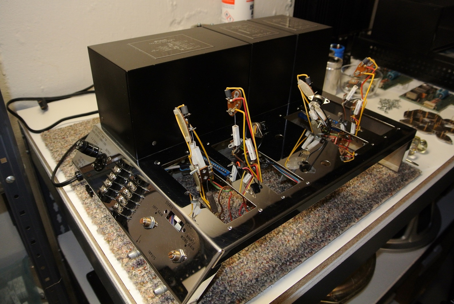
This page discribes a replacement two-stage preamplifier input section for the first generation solid state McIntosh amplifiers. Specifically, I'm referring to the input section PC board part number 043-795 which is common to the MC2100, 2105, 2505 and 250 quasi-complimentary amplifiers. Having seen a few of these amplifiers in need of a new preamplifier PC board, it seemed appropriate to consider designing a new one. Rather than making a copy of the factory design however, a few design modifications were incorporated to improve the already excellent performance. Here, a complete overhaul of an MC2100 is performed including installation and test of the new preamplifier section identified as the R2 preamplifier.
FACTORY PREAMPLIFIER DESIGN
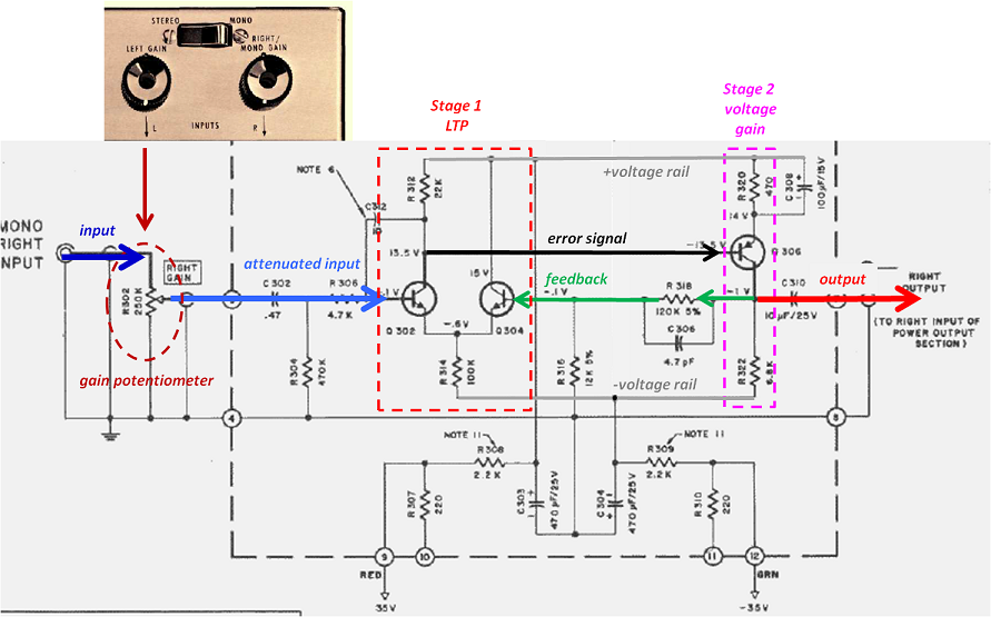
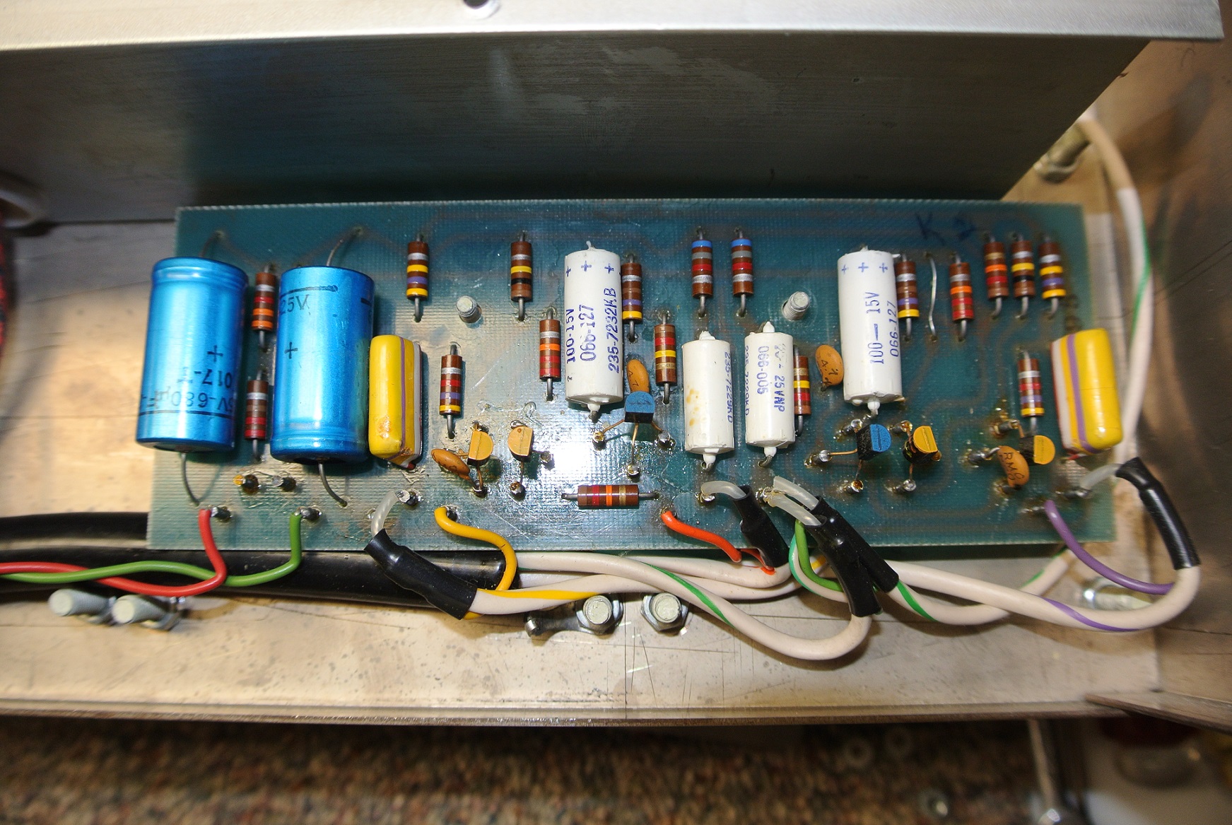
There were three schematics published over the production history of the amplifier with the last one being part number 380-948. The factory design input section is a two-stage preamplifier. One channel is shown below (the power supply section is common to both channels). The first stage, highlighted in red, goes by names like long-tailed pair (LTP), emitter coupled amplifier or a differential input, single ended output amplifier. Regardless of its name, its a transconductance amplifier that outputs a current signal that's a function of the differential input voltage across its bases. The LTP consists of two matched, emitter coupled, NPN transistors Q302 and Q304. The input signal is applied to the base of Q302. Feedback is applied to the base of Q304. The output from the LTP is taken from the collector of Q302; its collector loaded by a 22k load resistor R312 and, in parallel, the input impedance of PNP voltage gain stage Q306 (highlighted in fuschia). The tail current of the LTP is determined by the voltage drop across R314. Local negative feedback is provided by sensing the collector output of Q306, attenuating the amplitude of the signal by the resistor pair R318 and R316 and routing the attenuated signal to the base of Q304. Compensation is applied by capacitor C306. The magnitude of the current signal from the collector of Q302 is proportional to, and 180° out of phase with, its base-emitter voltage difference. The current waveform at the collector of Q302 is referred to as the error signal and it drives the voltage gain stage of the preamplifier.
R308, 309 determine the rail voltages and can differ from what's shown in the schematic. The easy way to determine the values for your amplifier (and presuming your amplifier is working without issue) is to read the magnitude from the color bands or measure them with a DMM. Typical factory values are 2.2k, 3.3k and 4.7k Ohms. The supply caps C303, 304 may differ as well.
THE NEW DESIGN
The R2 preamplifier is a drop-in replacement. Input and output impedances, closed loop gain, phase and gain margins, bandwidth, power supply burden load, layout of the input and output connections and mounting of the board to the chassis were all constraints considered in the design. The schematic for both channels of the R2 preamplifier is shown below. Experienced builders will immediately recognize the layout as a ultra-linear LTP input stage, capable of low distortion, sending an error signal to a Miller compensated, common emitter voltage gain stage.
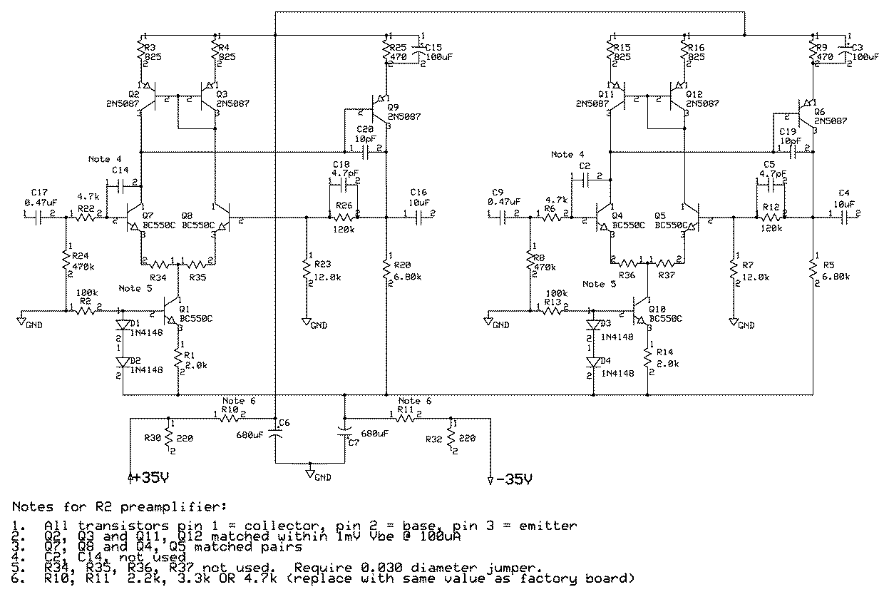
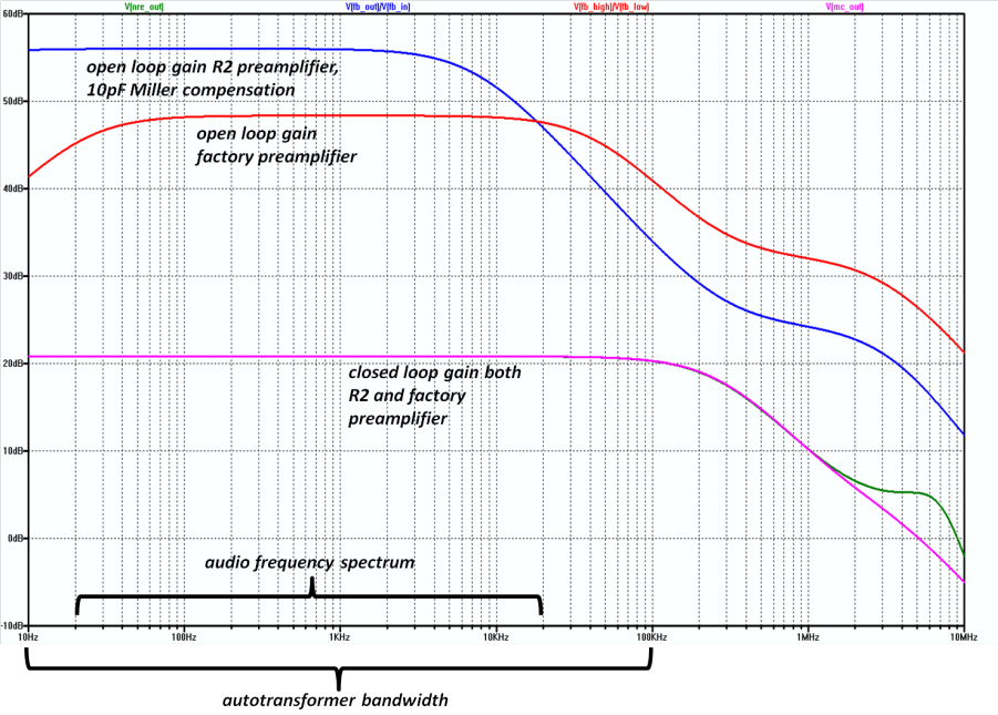
The R2 design makes the LTP work a bit harder by increasing its compensated, un-degenerated low frequency open loop gain which, for the same closed loop gain, means a greater fraction of the output subtracted from the input to thus further reduce contributions associated with the various voltage artifacts that act to distort the signal as it passes through the preamplifier. The collector load resistor in the factory design, R312, has been replaced by a current mirror and thus improving differential pair transconductance. By keeping the closed loop gain of the R2 preamplifier equivalent to the factory unit, simulation predicts low-frequency feedback applied by the R2 preamplifier is about 8dB greater than the factory design as is illustrated in the Bode plots of open and closed loop responses below. Closed loop gain for the factory design, based on actual measurement, is about 21dB (11x). Closed loop gain of the R2 preamplifier is set to be the same as that of the McIntosh design.
In the factory board the tail resistor, R314, provides a current sink that has been replaced with an active sink in the new preamplifier. The active sink improves transconductance linearity and common mode rejection ratio (CMRR). The performance improvement of adding the current mirror load and active current sink will be illustrated first by simulation and then, in the synthesis section, by measurement.
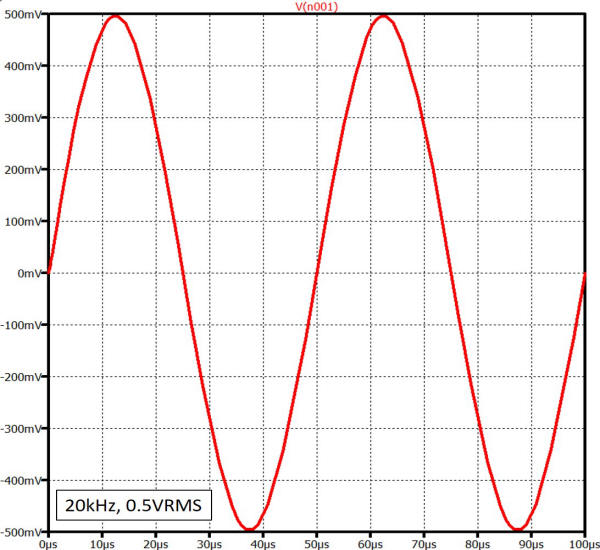
The first graph shown below is a plot of the simulated input signal used to determine the transfer function of the two differential input pair designs. The input signal consists of two 20kHz, 0.5VRMS amplitude sine wave cycles. The transfer functions of the R2 preamplifier (blue) and the McIntosh factory design (fuschia) are shown super-imposed on the adjacent graph. The y-axis represents the voltage difference (mV) between the bases of the differential pair, i.e. the differential voltage, whilst the x-axis is the collector current magnitude (mA) at the output. Thus, the plots represent the differential pair transconductance transfer functions. Given this is a simulated response, the discrete devices for both the designs are perfect matches.
As is evident by comparison, the R2 preamplifier evidenced significantly better linearity demonstrating a near constant transconductance through the progression of the input signal. Apparent in the McIntosh design, the response (an ellipsoidal loop) is clearly not linear with a transconductance that varies as the sine waves progress through time. This is a source of distortion that is lowered by using the R2 preamplifier.
![]()
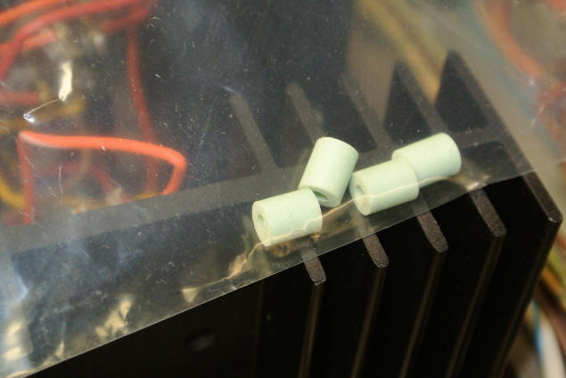
The simulations highlight the relatively low magnitudes of the differential input signals used in this stage of the amplifier thus negating the need to degnerate the emitters of the differential pair. The R2 PC board however has capability to add emitter degeneration resistors to the LTP (see resistors R34, R35 and R36, R37) allowing builders to design input stages to suit their specific design requirements. For the R2 preamplifier builds installed in the McIntosh amplifiers, 0.035in diameter jumper leads are soldered across the solder pads (see below).
SYNTHESIS
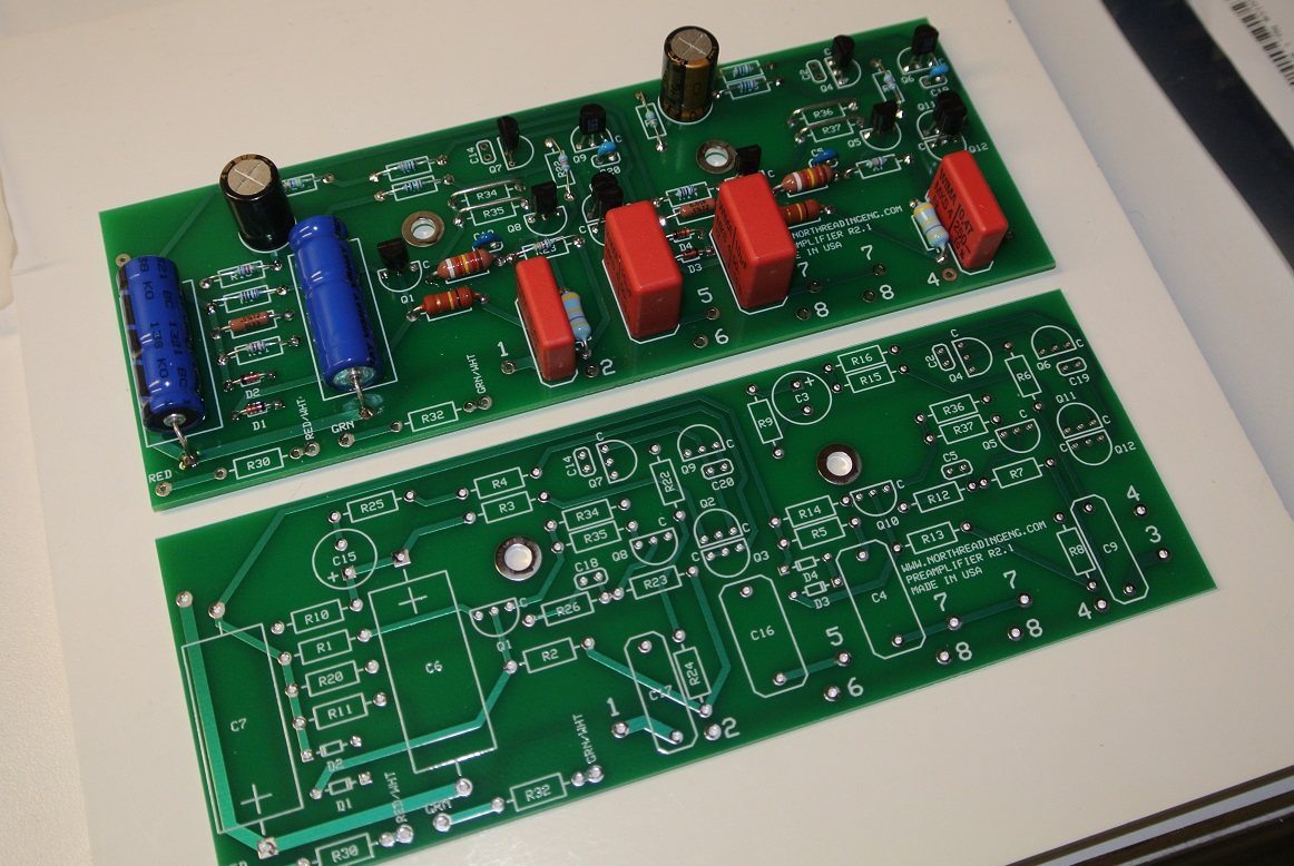
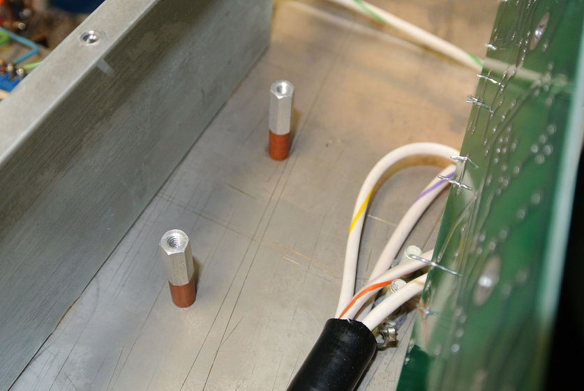
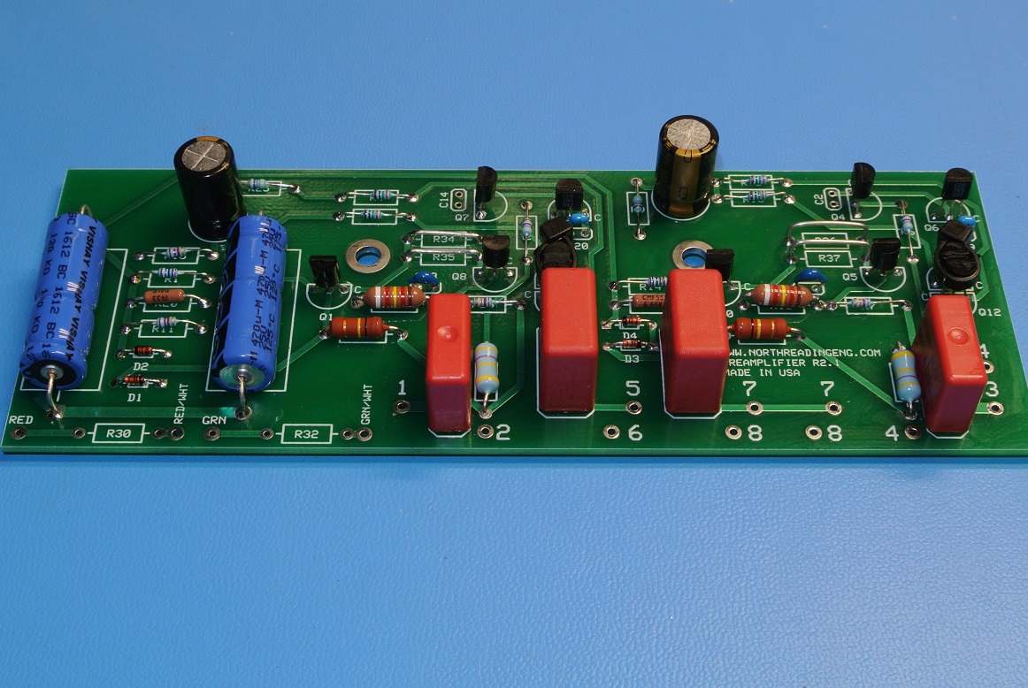
The 2-layer, PC board of the R2 preamplifier is shown below (left). The part IDs shown in the schematic (R2, C20, D4 and so on...) are silkscreened on the board. Although designed specifically for the McIntosh amplifiers listed above, the preamplifier is not limited to that application and, by suitable component selection, experienced builders will find the layout useful for amplifier builds that require a low distortion input stage based on discrete components. The boards are fabricated in the USA from 62mil thick FR-4 epoxy glass. Signal traces are wide at 40mils (supply rails and GND traces are 50mils) and trace thickness is 1.7mils (1 1/4 ounce copper plating). Copper adhesion is excellent and allows for numerous solder-unsolder cycles without solder pad lift off. All solder pads are plated on both sides and accommodate 35mil diameter leads. Wire to board inputs are 48mils in diameter. Resistors locations are sized for 0.6" lead spacing. To facilitate wire to board joining, the board is mounted to 1/2" tall stand-offs (see photo at right). The standoffs eliminate the need to use solder cups at the WTB joints.
The PC board, standoffs and mounting screws can be purchased from North Reading Engineering for your own McIntosh amplifier rebuild project. Matched transistor pairs for the current mirrors and differential pairs are also available. RoHS compliant boards can also be provided.
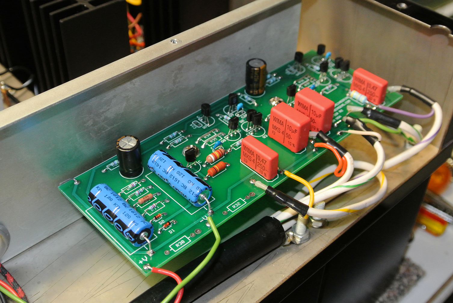
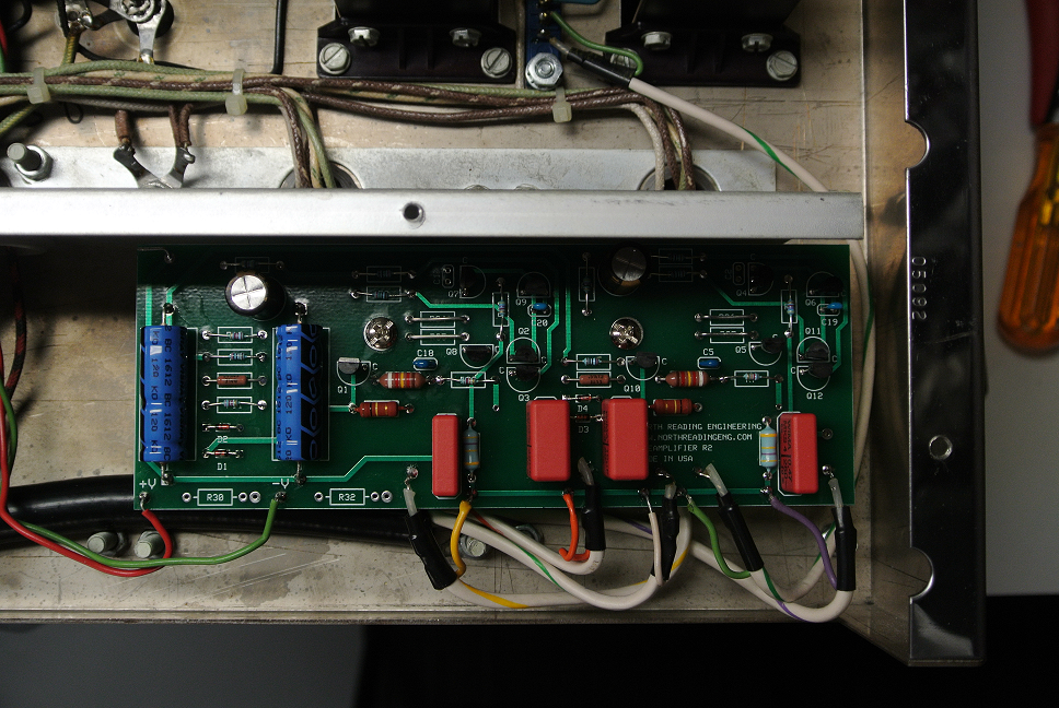
Below is an example of the R2 preamplifier installed in an MC2100. Note R30 and R32 are for amplifiers with blue meters and not used in the utility amplifier configurations (MC2100, MC250). All resistors are 1/2 or 1W film type.
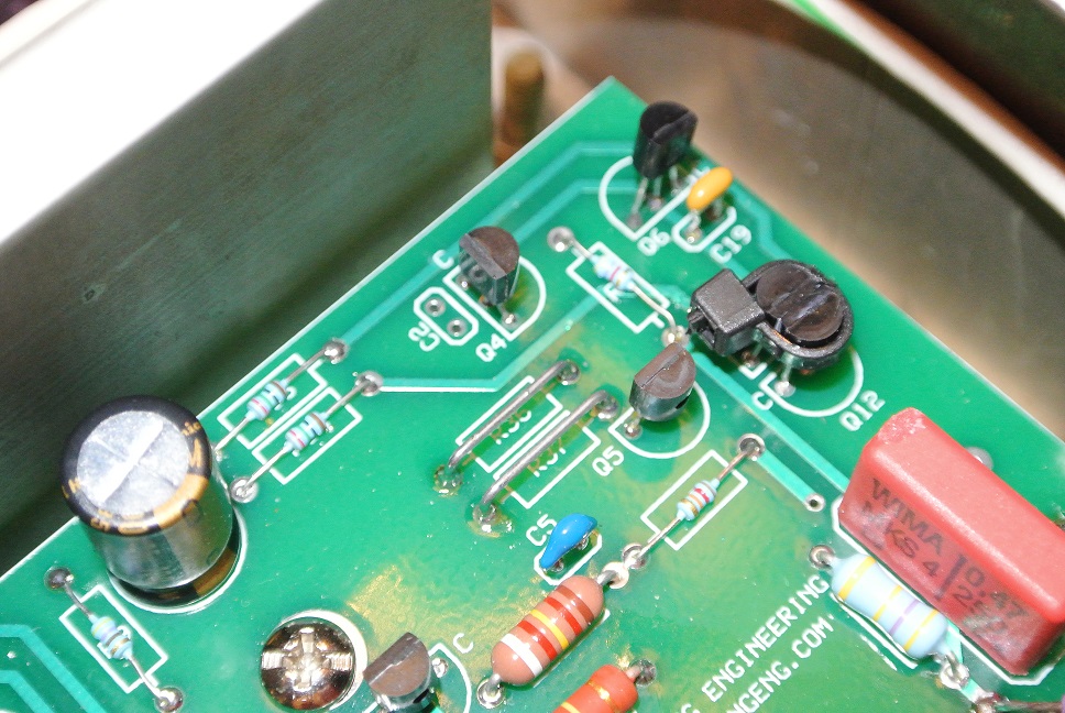
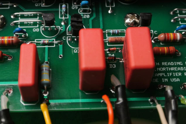
Jumpers bypass the emitter degeneration resistor locations provided on the board which, for the low differential input signals in the R2 design, make emitter degeneration unnecessary. To facilitate board assembly and troubleshooting, the collector pin is identified at each T0-92 location. The T0-92 lead spacing is designed for standard bent lead configuration (you can bend straight leads to fit too). Capacitor C20 (light blue) is Miller compensation, C18 is feedback lead compensation and C14 (not used) allow for input compensation. The compensation capacitor locations are all sized for 100mil lead spacing. Here, I've used MLCC type 1. The transistor pair Q2, Q3 is a current mirror. Thermal differences between the transistors can be minimized by physically joining the two devices at the flats using a small tie-wrap. Thermal grease at the joint helps too. In the performance plots below, the current mirror transistor pairs were Vbe matched to within <1/2mV difference at 100mA collector-emitter current.
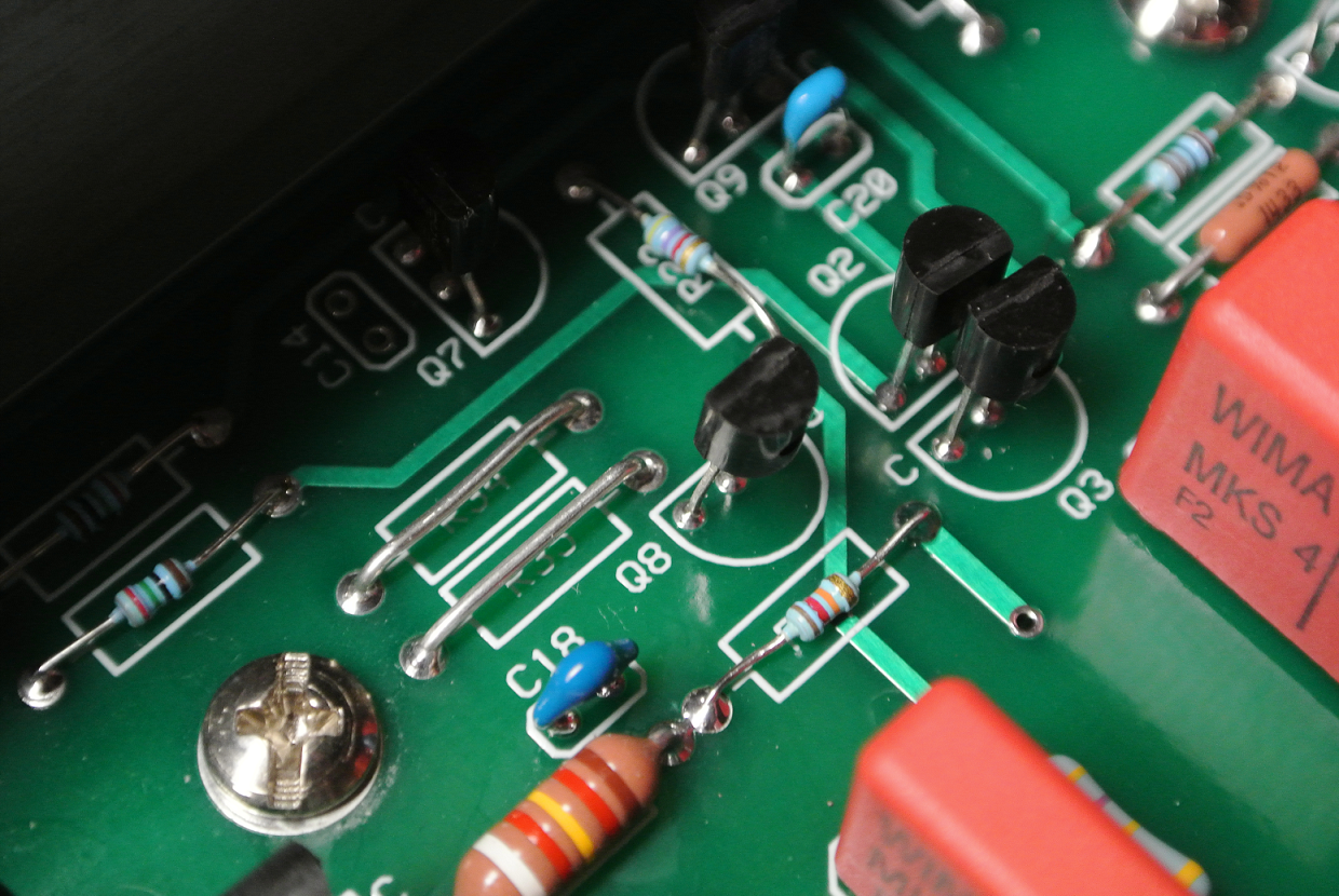
A comparison between the R2 preamplifier (right) and factory preamplifier (left) used for testing. Referring to the McIntosh preamplifier, the yellow paint on the factory T0-92 packages identify the differential input pairs, the blue ones are the voltage output stages. The yellow capacitors (with strips) are 0.47uF input coupling caps. The McIntosh preamp was not modified in any way from the factory components. Both input and output coupling capacitors in the R2 are WIMA with Teflon dielectric.
Component layout and trace routing for the R2 preamp is shown in the image below. Red traces are top traces, green are on the bottom. Although the solder pads have been sized to allow for easy visual inspection of joint wetting, I use a 10X loop to examine each joint for wetting and fillet examination.
MEASUREMENTS
Percent Total Harmonic Distortion (%THD) measurements were made using a Krohn-Hite 6900B Distortion Analyzer with factory, NIST traceable, calibration and a 24-bit CLIO FW audio analyzer. The CLIO unit is operating under Win7 Pro and interfaced using an IEEE 1394a Firewire PCI express adapter card with Texas Instruments chipset.
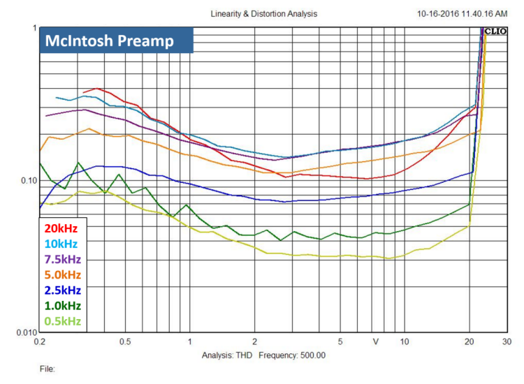
The first two plots below show the CLIO derived %THD as a function of output stage voltage swept from 0.20 to 24V at six test frequencies. The distortion is measured without filters using an FFT sampling rate of 192kHz resulting in all harmonics to 80kHz (Nyquist limit) being included. Filtering out harmonics above, say 30kHz will, of course, evidence lower distortion levels than shown here. The analyzer input was taken across a 4 Ohm, non-inductive, dummy load connected to the 4 Ohm output tap of the autotransformer. At the conclusion of testing the R2 preamplifier, the Variac was turned off, the R2 removed and the McIntosh preamp board installed. The CLIO analyzer remained on during the swap. The input gain pot was set at full. Both plots represent the left channel output.
Below the McIntosh factory distortion plot is the R2 preamplifier installed using the same test setup and test conditions. In that plot, the max distortion level measured from the McIntosh test is super-imposed over the R2 response (dashed line).
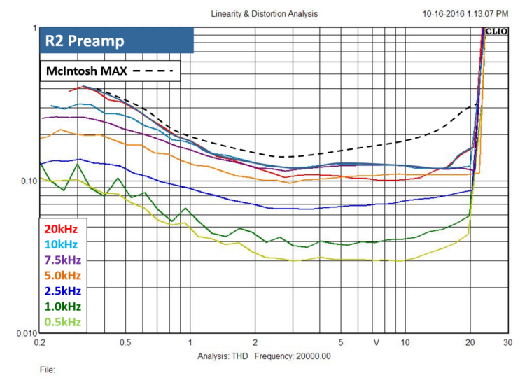
As is evident in the comparison, the largest reduction observed in %THD is at voltage levels greater than about 1V at the speaker load. Simulation predicts greater negative feedback at the mid-band frequencies. Based on the %THD measurements, the predicted behavior is realized in the measurements. Thus, improving the preamplifier open loop gain is an effective strategy to reduce distortion in amplifiers with this topology (i.e. quasi-complimentary outputs).
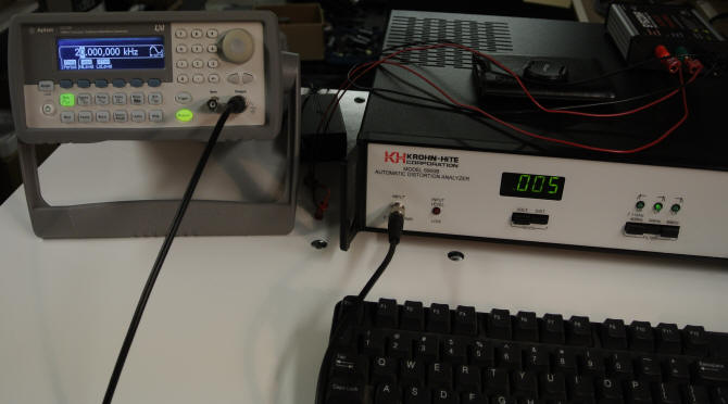
The Krohn-Hite 6900B is a fully automatic analog distortion analyzer that measures %THD between 3Hz and 1MHz. Distortion can be measured to as low as 0.005% between 5Hz to 50KHz with 0.001% resolution. The 6900B will also measure AC voltage magnitudes across its input from 100mV to a respectable 130Vrms(!). An ultra-low distortion 1kHz sine wave source with 0.002 %THD is provided by the instrument for calibration and amplifier distortion characterization. The absolute best feature of the 6900B however is that you don't have to fiddle with it, it's auto frequency nulling, auto input leveling and the meter auto-ranges to boot! An Agilent 33210A Arbitrary Waveform Generator was used to provide 20kHz signal for high frequency analysis. The 33210A provides a 20kHz sine wave signal at 4.0Vrms with 0.005 %THD.
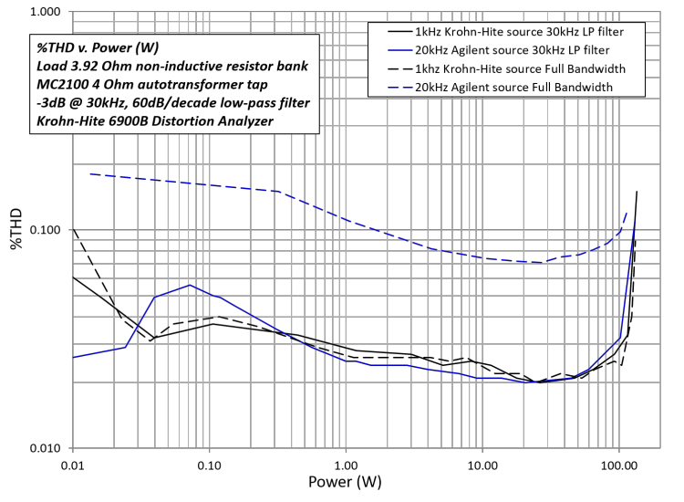
In the plot below the %THD of the amplifier at 1kHz and 20kHz is shown both with a low-pass filter (-3dB @ 30kHz with 60dB/decade roll-off) and without. The low-pass, which allows for the third harmonic of a 10kHz signal to be measured, reduces the effects of high frequency noise above the threshold of audibility. Thus, the magnitude of %THD with the filter engaged (solid lines) represents the distortion within the audible frequency range and, as evidenced in the plot, audible distortion is quite low. Note that a small reduction in the audible distortion shown in the plot below is possible by updating the complimentary power transistors on the power output board to the last configuration used by McIntosh (2N5322, 5320). Replacing the boards is discussed here.
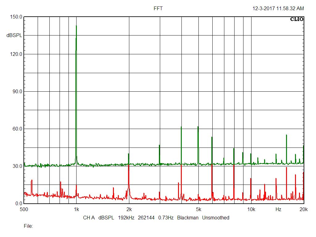
The typical preamplifier FFT is shown below. Green plot plot is FFT of a 1000Hz, 1VRMS amplitude signal applied to the input, no load across the output. In this measurement %THD is below 0.010. The red FFT is the preamplifier output with no signal. Distortion free dynamic range is about 84dB.
Stability is assessed using two approaches. First approach is to use square wave inputs at various frequencies to examine the output voltage at the transistor pins for evidence of high frequency ripple in the scope trace. The second approach utilizes high a spectral energy input signal such as a continuous MLS or Log Chirp and examine the frequency response for evidence of instabilities such as gain peaking which over time will cause the amplifier to overheat. At first use of the amplifier, monitoring heat sink temperature using a hand-held IR thermometers is also informative.
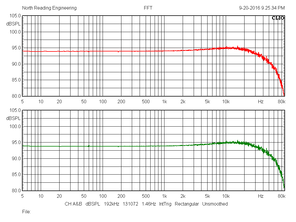
The frequency response of both left and right channels of the MC2100 test amplifier with the R2 preamp are shown below. Power levels near 100W/channel evidenced no significant deviations from the response uniformity shown below (5Hz to 20kHz within ~2dB). Measurement parameters: FFT bin size 131072, sampling rate 192kHz, 128k MLS test signal, frequency resolution 1.46Hz. Note the Nyquist limit of sampling rate limits the response to 80kHz.
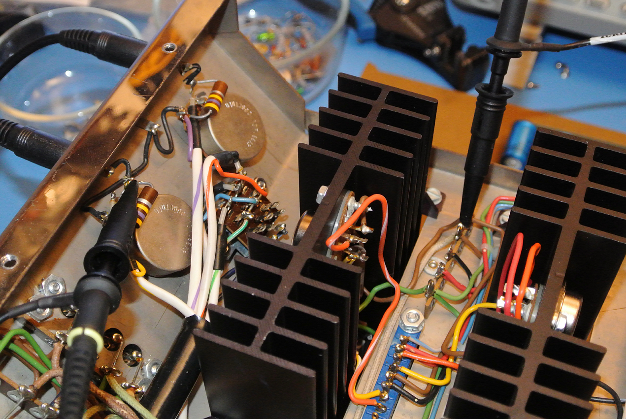
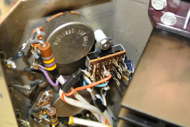
Square wave signals, measured at full output power using 1kHz, 10kHz and 20kHz test frequencies were analyzed for stability and oscillation. Measurements were taken with 10pF Miller compensation and 4.7pF feedback lead compensation. Probe locations for the tests are shown in the photo below. One probe is sensing the signal at the RCA input jack ahead of the gain input potentiometer. The second probe is sensing the voltage signal from the the output stage transistor pins (i.e. autotransformer input lead).
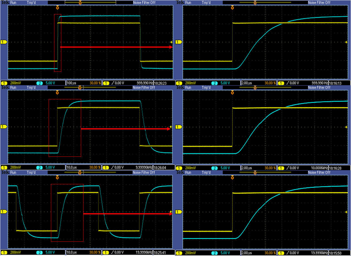
Scope screen captures at the test frequencies specified are shown below. Yellow trace (200mV/div) senses input signal measured at the input pin of the amplifier gain knob, blue trace (5V/div) is output voltage measured at output transistor pins. On the left side, the entire waveform trace is shown for each frequency. The windowed region of the waveform on the left is shown on the right. As is evident in the screen captures, no oscillations in the output waveforms are present. Phase margin of the R2 is 45°. The output traces are captured at extreme power (nearly 30Vrms across 8 Ohms).
AMPLIFIER OVERHAUL
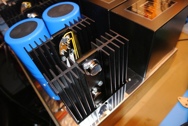
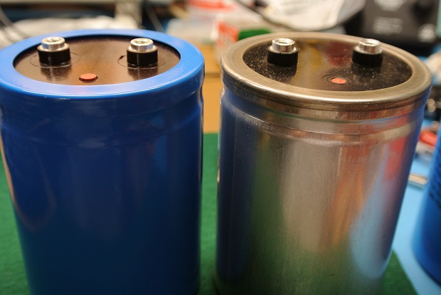
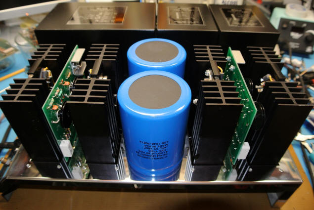
The MC2100 output stage and power supply were reworked prior to preamplifier testing. The output transistors, emitter resistors and power filter capacitors were replaced with new hardware. The heat sinks were removed and washed. The composition resistors on the original power output boards were measured and replaced where necessary. For the sake of appearance, the chassis was buffed using billiard cloth loaded with sub-micron diamond paste. When testing was completed the power output boards were replaced with new, factory units resulting in its own set of complications discussed here. Note that the changes that occurred over the long production run of the amplifier were largely confined to the power output boards.

SUMMARY
If you have interest in replacing your preamplifier with the R2 design shown above the PC board, aluminum standoffs and mounting screws are available for purchase. Please note however there are risks and potential dangers associated with working with voltages present in high power audio amplifiers. The use of grounding wands, grounding straps and ESD sensitivity should not be new concepts to you. If you've never powered up an amplifier using a Variac with one eye on the current, you may wish reconsider taking on a project of this magnitude. An oscilloscope is an essential tool and absolutely necessary for determining amplifier stability. That said, should you decide to rework your amplifier with our board, you take responsibility for the outcome. This is not a project for a young player. All it takes in one part installed improperly and "pop" goes your amplifier. If you're unsure about doing the work yourself, I can certainly do it for you.
If you do decide to build the preamplifier, testing it prior to installation in the amp is critical. That requires a power supply capable of provided at least +/-40VDC and the ability to measure current draw within the mA range (the preamplifier draws about 6mA with no load). The preamplifier provides about 21dB of gain (11X). The board can be modified for other amplifier configurations to suit the builders specific needs.
PRICING
1. R2 Preamplifier Printed Circuit Board w/Aluminum standoffs, mounting hardware, parts list (you purchase parts, build, test and install in amplifier): $39.00
2. Assembled R2 Preamplifier assembly w/Aluminum standoffs, mounting hardware (you install in amplifier): $295.00
For additional information including having North Reading Engineering completely over-haul your vintage McIntosh amplifier click here.
REFERENCES
1. The Art of Electronics, 3rd Ed., P. Horowitz, W. Hill, Cambridge University Press, 2015 (P. 116)
This webpage and its contents are the property of John Warren of North Reading Engineering, North Reading, MA 01864 USA. No part of the above work may be copied and published, in part or in total, without written permission.
© 2017 John Warren